AFOSR-MURI
HyNANO: 3D Hybrid CMOS-Memristor Circuits, Architectures, and Applications
Sponsored by the Air Force Office of Scientific Research (AFOSR) through the Multidisciplinary Research Program of the University Research Initiative (MURI) program.
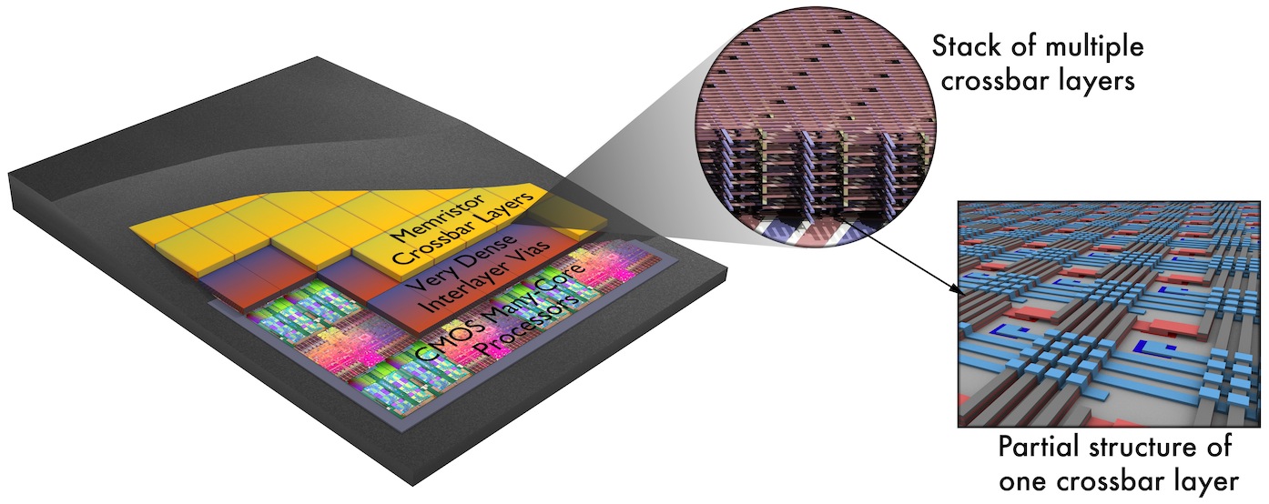
The objective of this multidisciplinary research project is to develop fundamentally new ways of advanced information processing based on monolithically 3D-integrated, hybrid CMOS/nanoelectronic circuits. These circuits will combine a CMOS subsystem with several layers of nanowire crossbars, with two-terminal “memristive” nanodevices at each crosspoint, all connected by area-distributed interfaces. This approach combines the advantages of CMOS technology, including its high flexibility, functionality and yield, with the extremely high density of nanowires, nanodevices and interface vias.
As a result, the 3D CMOS/nano hybrids will overcome limitations pertinent to other 3D integration techniques (such as through-silicon vias) and enable 3D circuits with unprecedented memory density (up to 1014 bits on a single 1-cm2 chip) and aggregate interlayer communication bandwidth (up to 1018 bits per second per cm2) at manageable power dissipation. Such performance represents a significant step towards addressing the most pressing needs of modern, compact electronic systems.
The project team members include the pioneers of the CMOS/nano hybrid approach and the experimentalists who have achieved the best results in the development of the most critical components of the hybrid circuits, in particular highly reproducible CMOS-compatible “memristive” crosspoint devices and their first integration with CMOS. A major focus of the project is optimization of these devices simultaneously with the 3D circuit integration using area-distributed interfaces, on a common CMOS base. This experimental work is proceeding in parallel with ab-initio and phenomenological theoretical simulations of memristive devices, aimed to improve the understanding of the fundamental physics of their operation. Simultaneously, we are developing and evaluating architectures of hybrid 3D circuits to utilize the advantages of such 3D integration in the most efficient way. Our research also include exploration of using such hybrid circuits as petabit-scale resistive memories, high-performance reconfigurable logic circuits, and bio-inspired mixed-signal systems for advanced information processing, such as pattern classification.
These separate thrusts will soon be combined into a single, joint effort towards a 3D hybrid CMOS/nano circuit demonstration, using the most advanced crosspoint device type, integration method, and the most promising system architecture. The goal is to make a sufficiently convincing demonstration to ensure easy transfer of this new technology to the electronics and defense industry.
This project also serves as the base for multidisciplinary research training of a large group of graduate students in one of the most exciting fields of nanotechnology.
